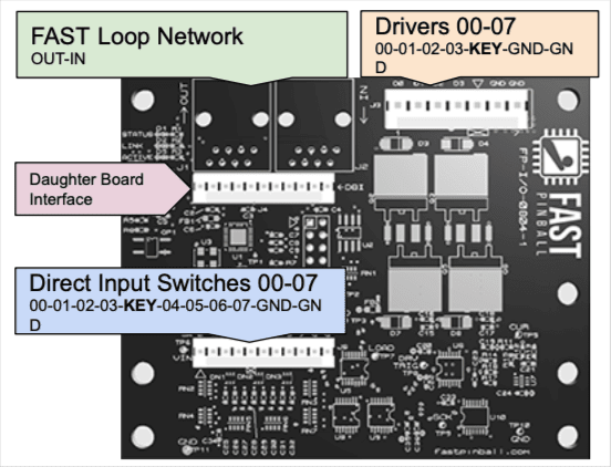
FAST Playfield I/O Board 0804
Part Numbers: FP-I/O-0804
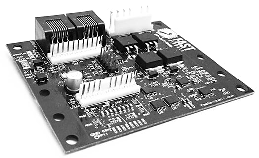
The FAST I/O 0804 is part of the FAST Modern Platform. It connects to the FAST Controller via the FAST I/O Loop. Each FAST I/O board is powered with 12v provided to the board using the RJ45 cables connected to the FAST Controller.
Note
The FAST Mondern Platform has various I/O Boards with different combinations of switch inputs and driver outputs. See the FAST Modern Platform documentation for details.
Features
- 8 direct switch inputs
- 4 driver outputs
Connectors
Connector Housings Needed
- 11 pin .100" Female Connectors
- 7 pin .156" Female Connectors
- RJ-45 CAT-5 Cables
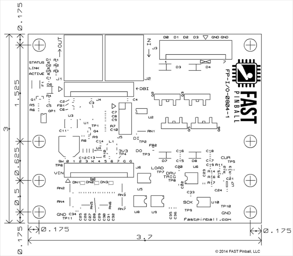
Mechanical Diagram
Dimensions are in inches.
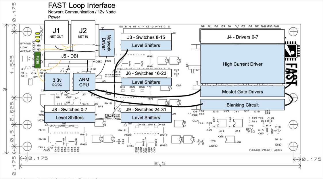
Block Diagram
Here's the block diagram for the 3208 driver board. It's the same for the 0804, the only difference is the number of switches and drivers it supports.
Status LEDs
There are 3 status LEDs on this board.
- STATUS is the processor status on this board. Slow flashing means everything is fine. Fast flashing means the board is inactive, which could include a watchdog timeout.
- LINK is on solid if this board can see its neighbor over the I/O loop and that everything is good. If this is off, then communication is not happening, which could mean there's a problem with the board, or the cable is bad or loose, or the neighboring board it's plugged into is bad.
- ACTIVE turns on (typically briefly) when a driver is currently active (e.g. it's actively firing) or a switch just changed state. This is great for testing. If a driver should fire and it doesn't, you can check to see if this LED flashes when the driver is supposed to fire. If yes, then you have a driver problem, if not, then it's a code or problem with the control system. You can also use this as a "local" switch test, as this LED should flash briefly when you activate a switch.
MOSFET / driver mapping
FAST I/O Boards use one MOSFET to control each driver output. If you connect something wrong and blow a FET, you can replace them easily. (Even though they're surface-mount, you can use a hot air gun and solder paste to replace them.) If you need to do this, here's a diagram which shows which MOSFETs control which driver outputs. You can verify you have the proper one by testing continuity between the MOSFET center pin and the driver output pin.

Replacement MOSFET part number is IRL540NSTRLPBF
Firmware Updates
FAST I/O Boards have microprocessors on them, which means they have firmware. The I/O 0804 board is compatible with both Neuron and Nano Controllers, though different firmware is used with each. There's a simple command to update from 1.x to 2.x firmware (when moving an I/O board from a Nano to Neuron system). It's possible to go "back" from 2.x to 1.x, but that's more complicated.
Check our firmware page to see the latest versions and learn how to update your boards if needed.
Wiring Guides
We have guides that cover I/O board wiring, switch wiring, and driver wiring which are all part of our larger FAST Pinball guide to wiring series.
Connectors Housings Needed
| Qty | Pins | Size | Description |
|---|---|---|---|
| 1 | 7-pin | 0.156" | drivers |
| 1 | 11-pin | 0.100" | switches |
Note that the 11-pin header labeled DBI (near the RJ-45 jacks) is no longer used (and may not be installed on your board). So that connector is not included in the table above. (This DBI functionality has been replaced by the FAST Expansion Bus.)
Connector Pinouts
| J1 | I/O Loop OUT | RJ45 – CAT5e/CAT6 | |
|---|---|---|---|
| 1 | COM ENABLE | OUTPUT | |
| 2 | GROUND | GROUND | |
| 3 | Fused 12v | OUTPUT | |
| 4 | COM- | OUTPUT | |
| 5 | COM+ | OUTPUT | |
| 6 | Fused 12v | OUTPUT | |
| 7 | GROUND | GROUND | |
| 8 | GROUND | GROUND |
| J2 | WIRE | I/O Loop IN | RJ45 – CAT5e/CAT6 |
|---|---|---|---|
| 1 | COM ENABLE | INPUT | |
| 2 | GROUND | GROUND | |
| 3 | Fused 12v | OUTPUT | |
| 4 | COM- | INPUT | |
| 5 | COM+ | INPUT | |
| 6 | Fused 12v | OUTPUT | |
| 7 | GROUND | GROUND | |
| 8 | GROUND | GROUND |
| J3 | PIN | Driver Bank – 0-7 | 1×12-Pin .156″ |
|---|---|---|---|
| D0 | Driver 0 | OUTPUT | |
| D1 | Driver 1 | OUTPUT | |
| D2 | Driver 2 | OUTPUT | |
| D3 | Driver 3 | OUTPUT | |
| K | KEY | N/A | |
| D4 | Driver 4 | OUTPUT | |
| D5 | Driver 5 | OUTPUT | |
| D6 | Driver 6 | OUTPUT | |
| D7 | Driver 7 | OUTPUT | |
| GND | High Voltage Ground | INPUT | |
| GND | High Voltage Ground | INPUT | |
| GND | High Voltage Ground | INPUT |
| J4 | PIN | Driver Bank – 8-15 | 1×12-Pin .156″ |
|---|---|---|---|
| D8 | Driver 8 | OUTPUT | |
| D9 | Driver 9 | OUTPUT | |
| D10 | Driver 10 | OUTPUT | |
| D11 | Driver 11 | OUTPUT | |
| D12 | Driver 12 | OUTPUT | |
| K | KEY | N/A | |
| D13 | Driver 13 | OUTPUT | |
| D14 | Driver 14 | OUTPUT | |
| D15 | Driver 15 | OUTPUT | |
| GND | High Voltage Ground | INPUT | |
| GND | High Voltage Ground | INPUT | |
| GND | High Voltage Ground | INPUT |
| J6 | PROGRAMMING | 2×5-Pin .100″ | |
|---|---|---|---|
| Device Programming | INPUT/OUTPUT |
| J7 | PIN | Switch Bank – 0-7 | 1×11-Pin .100″ |
|---|---|---|---|
| 0 | Switch 0 | INPUT | |
| 1 | Switch 1 | INPUT | |
| 2 | Switch 2 | INPUT | |
| 3 | Switch 3 | INPUT | |
| K | KEY | N/A | |
| 4 | Switch 4 | INPUT | |
| 5 | Switch 5 | INPUT | |
| 6 | Switch 6 | INPUT | |
| 7 | Switch 7 | INPUT | |
| G | Switch Return Ground | OUTPUT | |
| G | Switch Return Ground | OUTPUT |
| J8 | PIN | Switch Bank – 8-15 | 1×11-Pin .100″ |
|---|---|---|---|
| 8 | Switch 8 | INPUT | |
| 9 | Switch 9 | INPUT | |
| 10 | Switch 10 | INPUT | |
| K | KEY | N/A | |
| 11 | Switch 11 | INPUT | |
| 12 | Switch 12 | INPUT | |
| 13 | Switch 13 | INPUT | |
| 14 | Switch 14 | INPUT | |
| 15 | Switch 15 | INPUT | |
| G | Switch Return Ground | OUTPUT | |
| G | Switch Return Ground | OUTPUT |
N or > jump the next page, P or < for previous, search with S or ?